
FAQs
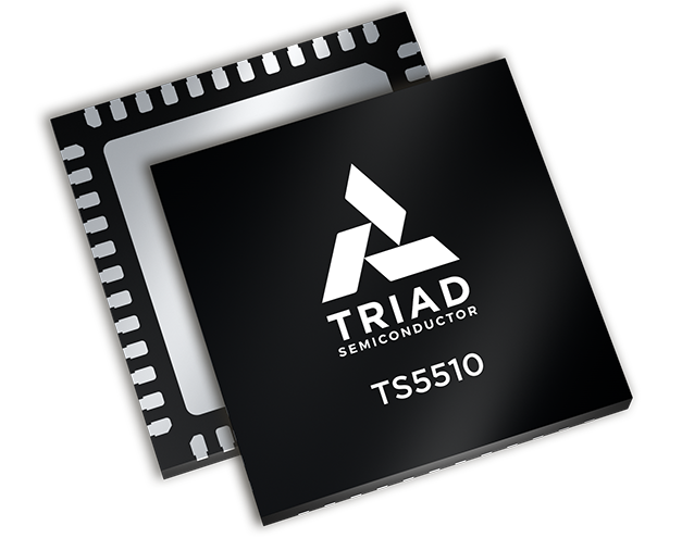
TS5510
Architecture and Performance
What is the fundamental difference between the TS5510's internal Current Conveyor topology and a traditional Instrumentation Amplifier (INA)?
How does the TS5510 achieve 'Universal Voltage Compliance'?
What does 'ADC Agnostic' mean, and why is it important for my design?
How does the TS5510 eliminate audible 'clicks and pops' during gain adjustments?
Design and Integration
What components can the TS5510 eliminate from my Bill of Materials (BOM)?
The TS5510's high integration dramatically reduces the external component count. It eliminates or incorporates:
- Precision gain-setting resistor networks (gain control in 1dB steps is on-chip)
- Optimized audio ADC driver
- Output DC removal
- ADC overload protection and mid-point bias
- No external resistive pad for high amplitude input signals
- High input impedance can reduce physical size of input capacitors
This consolidation is contained in a tiny physical footprint (7mm x 7mm package) and reduces component tolerance, charge injection and thermal drift issues inherent in discrete solutions.
Is the TS5510 suitable for both professional audio and industrial sensor applications?
Yes, absolutely. The core architectural advantages—class-leading CMRR, high CM voltage tolerance, and seamless gain control—solve the fundamental signal integrity problems common to both domains:
- Audio: High-fidelity microphone preamps requiring wide gain ranges and click-free switching
- Industrial/Sensor: Interfacing microvolt-output sensors over long cables in noisy environments (high CM interference) and allowing the required signals to be digitized reliably
How is the TS5510 controlled? Is it analog or pin programmable?
The TS5510 processes the analog input signal but is digitally controlled. Gain and attenuation settings are managed via an industry-standard digital interface (SPI) to command the internal switching network, Zero Cross Detect logic and GPIOs. This allows for precise, repeatable, and remote gain control.
What are the primary advantages of the Current Conveyor based architecture in terms of development time?
The TS5510 significantly reduces development time in two main ways:
- Eliminating Iterative Analog Design: The integrated, high-performance AFE is robust, eliminating the need for engineers to spend weeks or months fine-tuning discrete resistor networks or complex analog circuits to manage noise and common-mode interference. The TS5510 is simpler and more repeatable to duplicate across product lines with different PCB layouts and physical constraints.
- Simplified ADC Interface: Its ADC-agnostic nature and robust output drive simplify the interface to the ADC, reducing the complexity often found when matching proprietary AFEs to converters.
Can I defeat the DC servo function?
Yes, the DC servo feature can be disabled. This may improve click/pop artefacts at high gain settings in some applications. This is accomplished by shorting DCS1 to CML1 (channel 1), and by shorting DCS2 to CML2 (channel 2). No other audio parameters are affected by this modification.
Do any of the external support components require specific attention or selection?
As with any amplification system capable of high gain, care should be taken in support component selection and placement. SM ceramic capacitors with certain dielectrics can exhibit microphonic affects that can translate mechanical movement into electrical signals. Triad Semiconductor recommends that the capacitors on the DCSx and CMLx pins should not be surface mount with X5R, Y5V or similar dielectrics. High quality dielectric or leaded components should be used on these pins.
Similarly, any capacitors in the signal path need to perform well. The high inherent input impedance of the TS5510 allows smaller value input caps to be chosen, meaning non-electrolytic capacitor types could be considered.